|
Cleanroom |
|
|
|
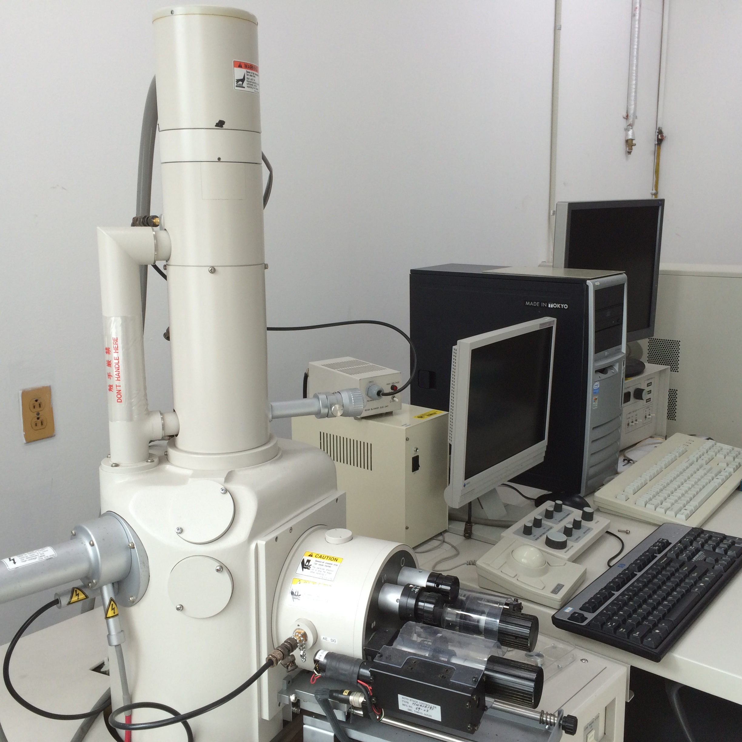
Scanning electron microscope & E-beam lithography system
A scanning electron microscope (SEM) is a type of electron microscope that produces images of a sample by scanning it with a focused beam ofelectrons. The electrons interact with atoms in the sample, producing various signals that can be detected and that contain information about the sample’s surface topography and composition. Electron-beam lithography (often abbreviated as e-beam lithography) is the practice of scanning a focused beam of electrons to draw custom shapes on a surface covered with an electron-sensitive film called a resist (“exposing”).[1] The electron beam changes the solubility of the resist, enabling selective removal of either the exposed or non-exposed regions of the resist by immersing it in a solvent (“developing”). |
|
|
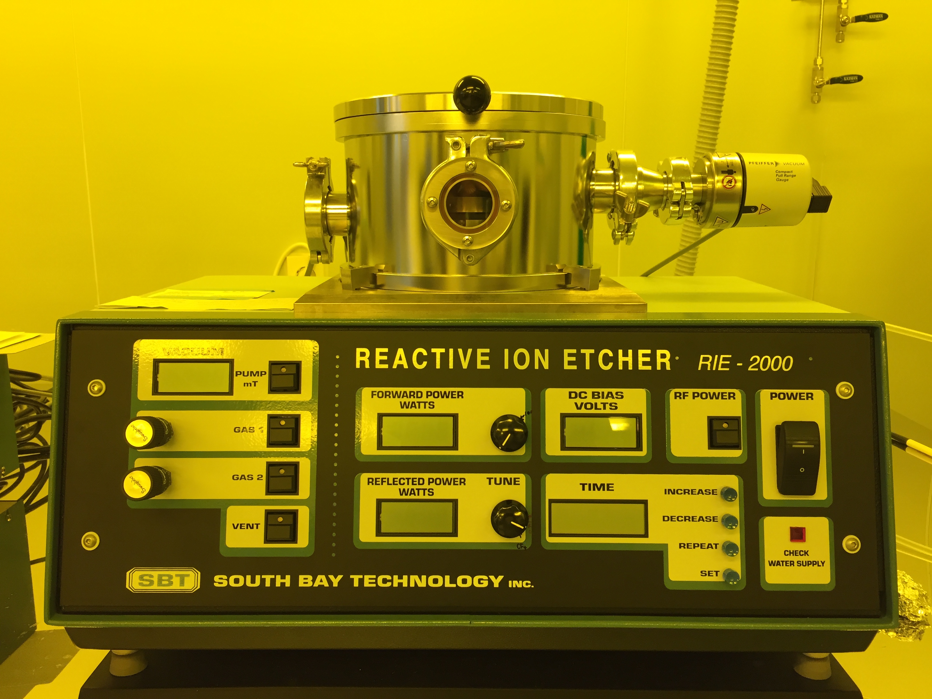
Reactive Ion Etching system Reactive-ion etching (RIE) is an etching technology used in microfabrication. RIE is a type of dry etching which has different characteristics than wet etching. RIE uses chemically reactive plasma to remove material deposited on wafers. The plasma is generated under low pressure (vacuum) by anelectromagnetic field. High-energy ions from the plasma attack the wafer surface and react with it. |
|
|
Optical microscope
Optical microscope is type of microscope using visible light. The image from optical microscope is captured by CCD (Charge-Coupled Device) camera and send digital image to computer to analyze image. By various lens (from x5 to x100 objective lens), we can find very small size samples to several micrometers. Also we can transfer layer sample to another substrate on optical microscope stage. |
|
|
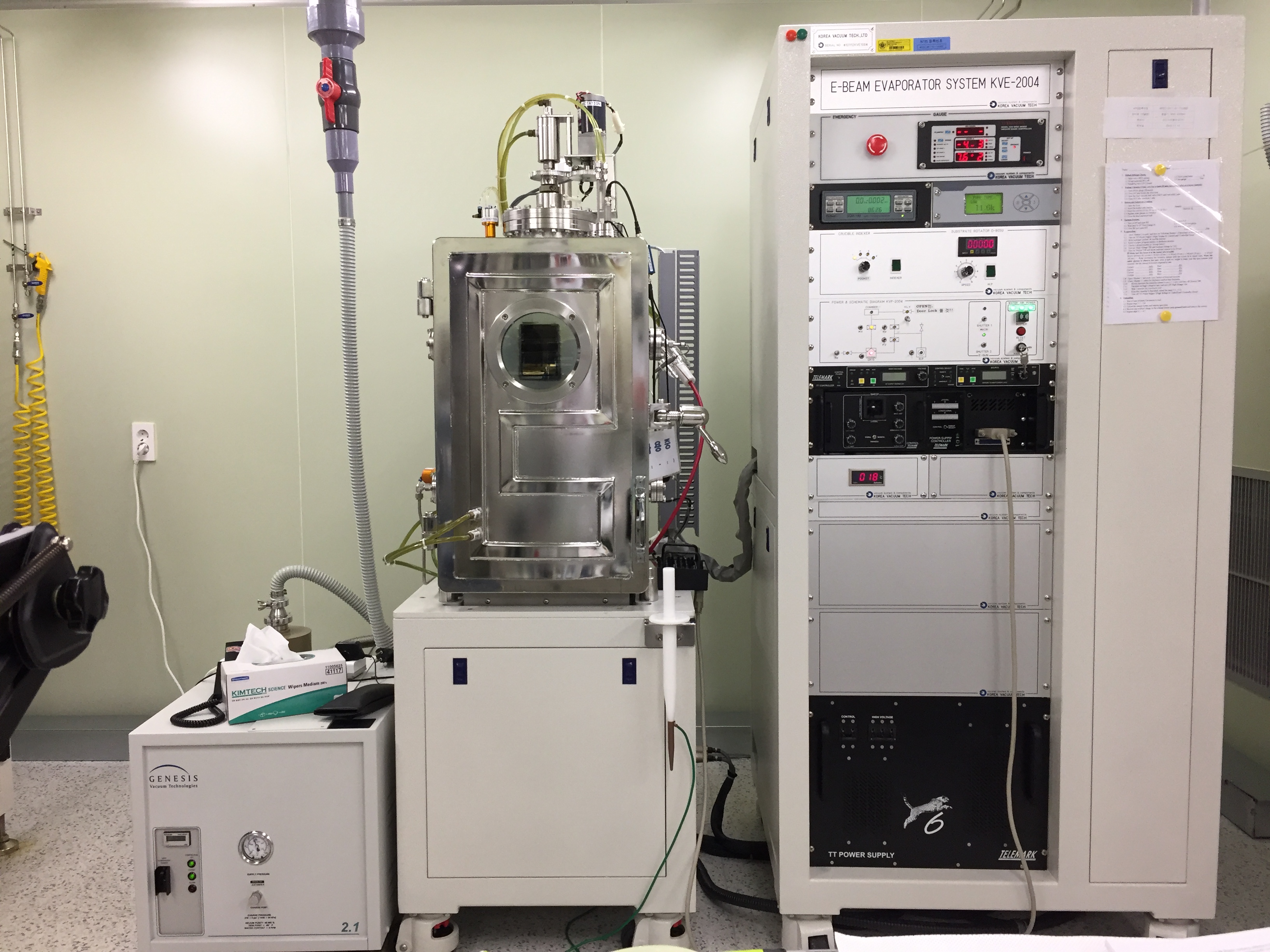
E-beam evaporator
When current flows in hot filament as a electron beam source, electron beam is generated. Electron beam is controllable using electromagnet by Lorentz force. Source materials(Au, Cr, Pd, Ti and etc.) collide with focused electron beam and it is enough heated to evaporate. A thin film is made of source materials on target substrates. Deposition speed and thickness are adjusted by controlling current flow rate and operating time, |
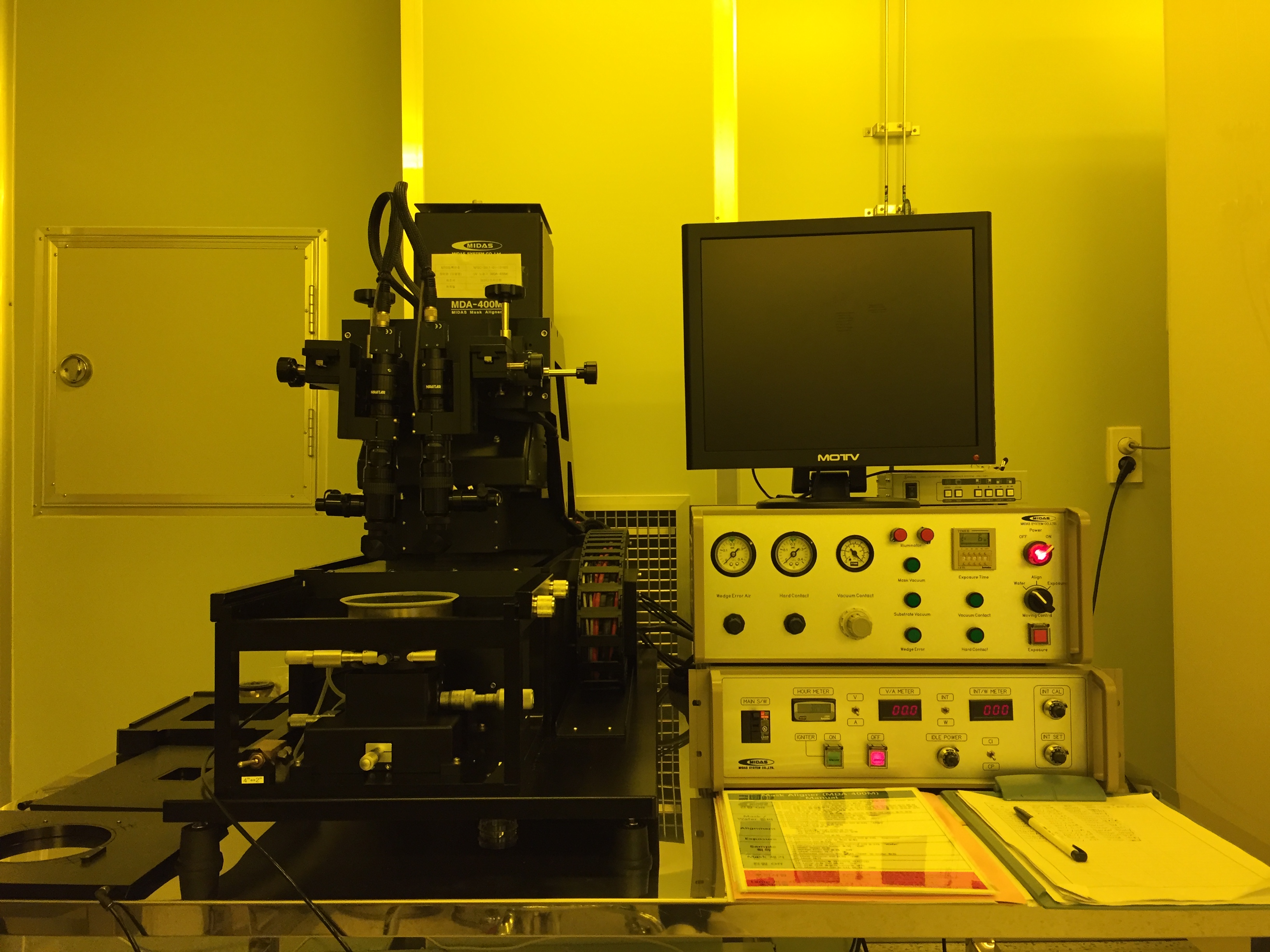 |
Mask aligner (Photo-lithography)
Photolithography is a process used in microfabrication to pattern parts of a thin film or the bulk of a substrate. It uses light to transfer ageometric pattern from a photomask to a light-sensitive chemical “photoresist” on the substrate. A series of chemical treatments then either engraves the exposure pattern into the material underneath the photo resist. |